Engineering Log: Tracking Down DP/VGA Heat in KVM-GO (and the Fix That Finally Worked)
Entry 1: The moment we realized it wasn’t “normal warm”
Midway through KVM-GO development, we saw thermal behavior that did not match typical “small device gets warm” expectations. It only showed up on two variants, DisplayPort (DP) and VGA. The HDMI variant stayed within expectations.
At first, the symptom was simple. The enclosure temperature became uncomfortable earlier than expected. What concerned us was not comfort. It was the possibility that internal temperatures were far above what consumer-grade components are meant to tolerate over time.
Entry 2: Why only DP and VGA
After tracing the video path design across versions, a pattern emerged.
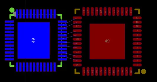
- HDMI: a single conversion stage (HDMI to USB video) using MS2130S
- DP: a two-chip chain (IT6563 plus MS2130S) to convert DP to USB video
- VGA: a two-chip chain (MS9288C plus MS2109S) to convert VGA to USB video
Two chips do not just add parts. They add power dissipation and localized hot spots. In a product sized like KVM-GO, those hot spots have very little room to spread.
Then we ran into the second constraint, surface area. KVM-GO pushes size to the limit, which means PCB area and effective heat-spreading area are both tiny.
Finally, there was a layout constraint that turned into a real engineering tradeoff. Placing both hot chips on the same side sounds ideal thermally, but the pinout and high-speed routing requirements made that approach difficult. Putting one chip more “inside” simplified routing and helped signal integrity, but it trapped heat in the interior of the enclosure.
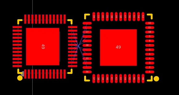
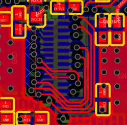
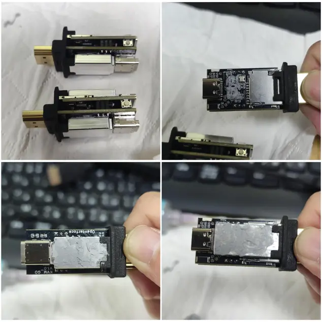
Original PCB layout
Original high-speed routing
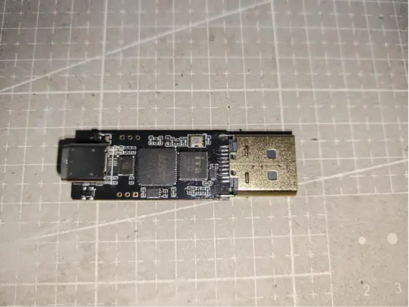
KVM-GO internal stack layout
Entry 3: Measuring what mattered, internal vs external temperature
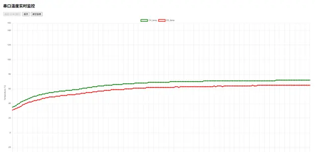
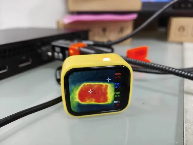
We decided to stop guessing and measure both sides of the problem. We built temperature measurement points for external and internal monitoring, then ran a long-duration workload test.
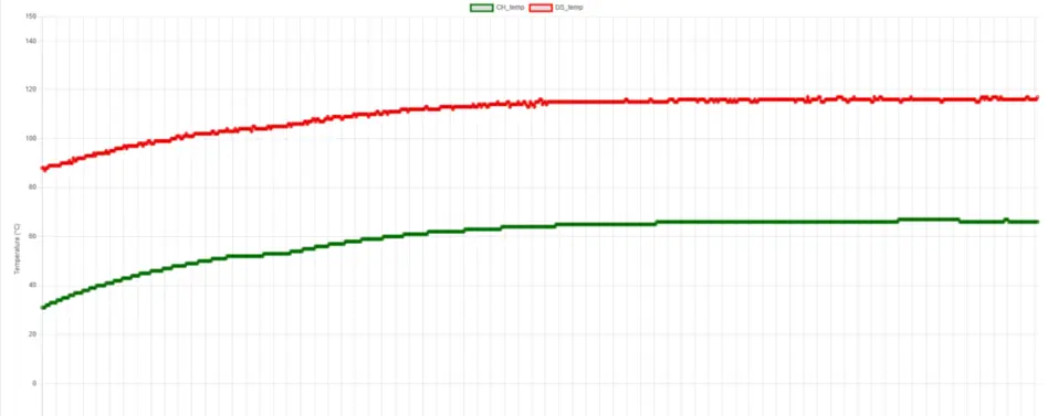
The result was alarming, especially on VGA.
After about one hour of sustained operation: - external surface reached about 65°C - internal temperature peaked around 115°C
Many consumer components are rated for maximum operating temperatures around 85°C, depending on the exact part and grade. Seeing triple-digit internal temperatures meant we were not just dealing with “hot to touch.” We were looking at something that could shorten product life or create unpredictable behavior across environments.
Baseline temperature test (internal vs external)
Entry 4: A quick sanity check, forced airflow works (but that’s not a product solution)
Before redesigning anything, we wanted a quick validation. If we can remove heat faster, do temperatures drop meaningfully?
We tried a simple forced-air setup using a DIY fan. It did what physics says it should. Temperatures dropped noticeably, roughly 15°C in our test. That confirmed the issue was a thermal bottleneck rather than measurement artifacts or software behavior.
It also confirmed something else. A fan is not compatible with the product we are building. KVM-GO needs to remain compact, silent, and self-contained. So forced airflow became a diagnostic tool, not the final answer.
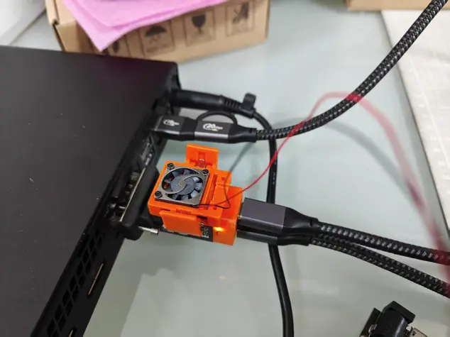
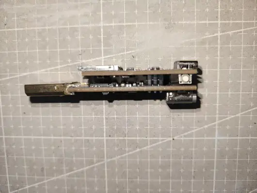
DIY fan cooling setup
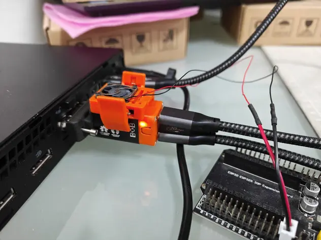
DIY fan cooling, alternate view
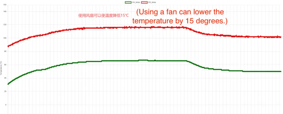
Temperature test with fan cooling
Entry 5: Fix step 1, move heat sources outward (without breaking signal integrity)
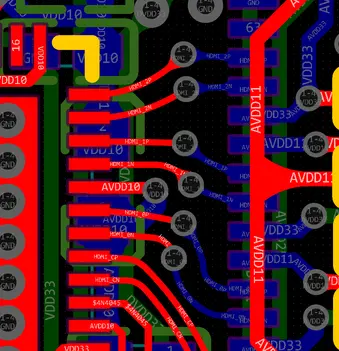
The first real fix was on the PCB. We pushed the design as far as we could toward placing both heat-generating chips closer to the exterior side.
This was not “just move the parts.” With DP and VGA, routing constraints are tight. Keeping the high-speed signals clean, especially the differential pairs, is non-negotiable. Putting both chips outward made routing harder, and we had to work carefully to avoid degrading signal integrity.
We compared old versus new layout and routing, then built hardware to verify behavior.
Revised PCB layout (chips moved outward)
Revised routing (pass 1)
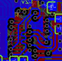
Revised routing (key area)
Revised PCB, built for validation
What changed after step 1
Thermals improved, but we spotted a second-order problem. Temperature still was not transferring effectively into the enclosure. Some areas stayed hotter than they should, and thermal imaging suggested the enclosure was not acting like a proper heat spreader.
Step 1 reduced peak heat stress, but it did not fully solve the heat path.
Temperature after layout change (step 1)
Shell heat transfer check (after step 1)
Entry 6: Fix step 2, build a real heat path (CNC aluminum blocks plus thermal interface)
At this point, we treated the enclosure as part of the thermal system, not just a cover.
We added: - CNC aluminum blocks on the upper and lower PCB stack - thermal interface material (thermal grease or pad) to couple heat into the aluminum and then into the aluminum enclosure
The goal was simple. Increase effective heat-spreading area and create a stable, low-resistance path for heat to reach the enclosure, where it can dissipate safely.
CNC thermal block (step 2)
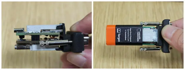
CNC block installed detail
Final result after step 2
After adding the conduction path: - external temperature stabilized around 65°C - internal temperature dropped to around 55°C
Thermal imaging showed what we wanted to see. Heat distribution became more even, and the enclosure finally participated in dissipating heat instead of letting it accumulate internally.
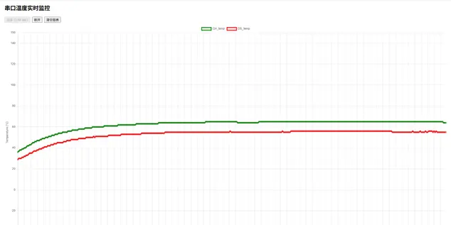
Temperature after CNC conduction (step 2)
Shell temperature after CNC conduction
Closing note
The takeaway from this issue was not simply “DP and VGA run hotter.” Multi-stage conversion costs more power and that part is expected. The real lesson was that in a device this small, where the heat goes matters as much as how much heat is generated.
Step 1 (layout) reduced internal hot-spot severity.
Step 2 (mechanical conduction path) made the solution durable and product-appropriate.
No fan, no special user handling, just a design that behaves predictably.